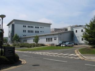
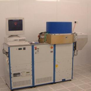
This equipment and the research staff are located in the Scottish Microelectronics Centre (SMC), a purpose built facility at the University's Science and Engineering campus at King's Buildings. The complex consists of approximately 250m2of class 10and 100m2of class 100 cleanrooms and 1000m2of office and laboratory space. It is a 200mm capable facility with the flexibility for processing smaller wafer sizes as well as chips and the SMC hosts both academic and industrial research operations. The facility focusses on smart microsystems technology and integration with a long track record of postprocess CMOS wafers (More than Moore technology).
Environment
The cleanrooms are located in the purpose build £4.2M Scottish Microelectronics Centre building. This class 10 facility comprises 250 sq metres is controlled to 21±1°C with a relative humidity of 40±5% with a raised floor being used as the air return to the plenum. Each bay is serviced with DI, town and chilled water, nitrogen, compressed air, power, gases and vacuum.
Wafer Fabrication Equipment
The Laboratories maintains the following major items of processing equipment:
- DC Magnetron Sputter Coater - Balzers BAS450 coater system with two 5 in × 10 inch targets presently used for coating up to 24 × 75mm wafer with Al/1%Si, Al,W and Ti. Ion beam pre-cleaning is available using an Ion Tec Inc Kafmann source
- Oxford Plasmalab System - 400 magnetron sputtering system capable of sputtering Al/1%Si, Al, W, Ta, Ti and TiN on up to 200mm wafers. Ion beam pre-cleaning is also available
- Diffusion Furnace Tubes - Three quad stack Tempress Omega L furnaces, upgraded to direct digital control with supervisor computer. The systems are tooled for 75mm wafers and support the following processes: 200mm tubes are available for oxidation, LPCVD silicon nitride (inc low stress) and polysilicon (inc low stress)
- Dry oxidation (with HCl gettering)
- Wet oxidation (burnt hydrogen with HCl gettering)
- Nitrogen anneals
- LPCVD of Polysilicon
- LPCVD of Silicon Nitride
- Dielectric Deposition
- STS Miultiplex PECVD vacuum load-lock system configured for SiOx and low stress nitride. Capable of coating up wafer diameters upto 200mm.
- Dry Etching
- STS PF 508 barrel reactor for plasma ash removal of photoresist
- STS Multiplex load locked aluminium and polysilicon RIE etcher using SiCl4, and Cl2 chemistry
- Plasmatherm Versaline DSE IV deep Si etch system
- STS Multiplex ICP - Load locked inductively coupled plasma etch system configured for deep Si etching
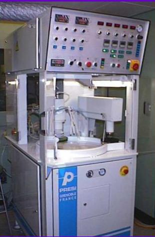
- Chemical Mechanical Polishing (CMP)
- Presi Mecapol E460 polisher
- Wet Etching - Fume extracted class 10 laminar flow chemical stations permit safe cleaning of furnace quartzware and the processing in industry standard cassettes through the stadard mineral acid cleaning and etching treatments. A Maragoni dryer is also available following rinsing.
- Wafer Lithography - Photoresist coating, developing and baking are achieved on 100mm SVG 8600 track system and a CEE 75-200mm coater/develop system each comprising:
- Dehydration bake/ vapour prime, coat, hotplate softbake
- Post exposure bake, spray/puddle develop, hotplate hardbake. Although facilities for negative resist processing are available, positive resist is the preferred patterning medium and the only one possible on the DSWs
- Spray coating of photoresist is also available (EVG 101)
- Lithography is performed using either amask aligner or projection system. The machines in use are:
- Karl Suss MA8 mask aligner
- Durham Magnto Optics Microwriter 3
- Both tools have backside alignmnet capability
In-Line Inspection and Measurement
Wafers are subject to visual inspection at all stages in processing using a variety of metallurgical microscopes from various manufacturers including Leitz, Reichart-Jung, Olympus, Leica DM12000 (optical IR, UV and 3D mapping) etc.
Access to SEMs, FIB and an AFM is also available
Profiling of wafer topography is available using a Dektak surface profilers to record step height variations in the range 0.01 to 1000 microns.
Dielectric layers and polysilicon layers are more readily measured using the Nanoscope Model 010-180 reflectometer.
Sheet resistance of large area process layers is measured using a Veeco 1000 4 point probe.
Wafer mapping nanoindentation is available (Keysight G200)
Assembly
A low volume capability for the assembly of chips into Flat Packs, TO5 and Dual In-line packages is available using the following equipment:
- Dicing Saw (DAD 640) - Disco 8" wafer chuck
- Wire Bond
- Disco 810 100mm wafer grinder
Off-Line Evaluation and Test
Parametric Testing
A HP4062UX test system with 48 switchable pins is connected to a Karl Suss 200mm PA200 automatic wafer prober with ProbeShield® EMC for low signal probing, which can be used to perform precision measurements (µV, fA) under software control. This system can also be used with temperature control up to 200 degrees C. Similar measurements may also be made using Keithley 4200 semiconductor parameter analysers and CV measurements on other manual probers. An RF probe system is also available for measurements of high frequency devices, including RF MEMS up to 3 GHz.
Device and Process Simulation
The Facility uses workstations running with the UNIX operating system to give multi-user access to the Synopsis process and device simulation packages. The following programs are available:
- TWB - Design of Experiments
- SUPREM-3 - 1-D Process simulation
- TSUPREM-4 - 1-D Process simulation
- MEDICI - 1-D Process simulation
- DAVINCI - 1-D Process simulation
- AURORA - Parameter extraction
- DEPICT - Photolithography
- TERRAIN - Etch and Deposition
- MICHELANGELO - Gridder and data display
- LAYOUT Mask - definition
- RAPHAEL - Capacitance/resistance calculations
- ICCAP - Parameter extraction
- RS/1 EXPLORE AND DISCOVERY - Design of Experiments
- CORNERSTONE - DOE and Statistical Analysis
Contact Email:
Address:
The School of Engineering, The University of Edinburgh,
Scottish Microelectronics Centre,
Alexander Crum Brown Road, Edinburgh, EH9 3FF


